Author: crackingcontraptions_3voi0v
The instructions require an STLINK/V2 ($21 and less off the web) which I don’t have of course.
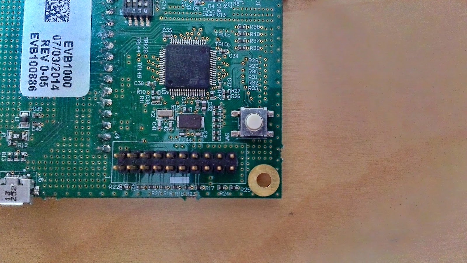
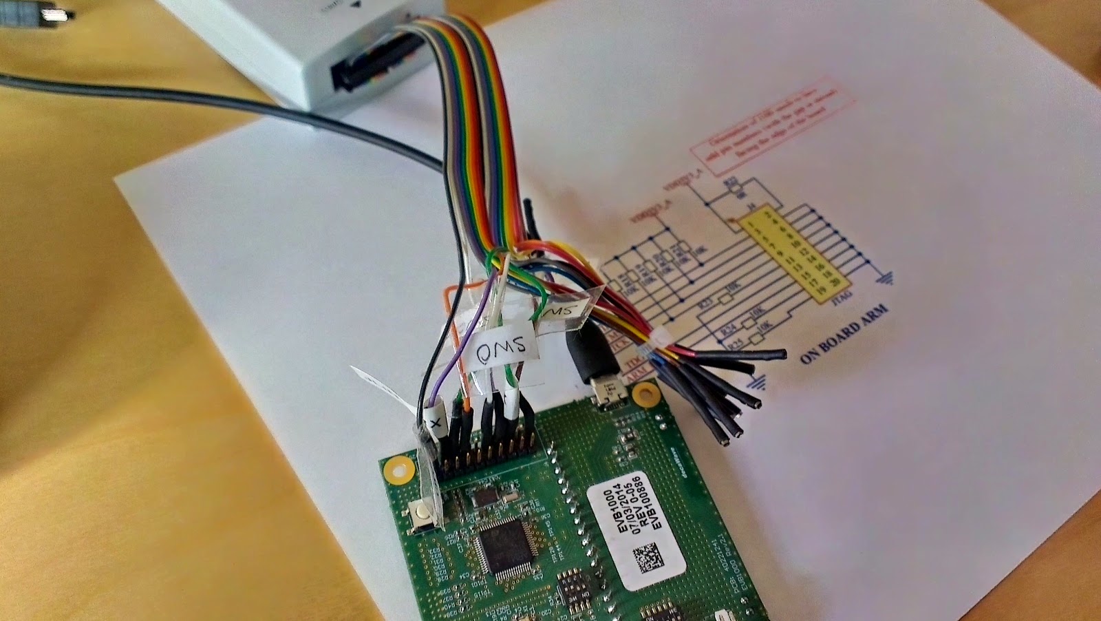
So can I use the JLink EDU. First challenge is getting the connector right. Which is pin #1?
I’ve written the canonical LED flasher program, but now I’m trying to figure out what port.pin the LEDs are on. Back to the Schematic…
timer_start(); blink_led_init();
// Infinite loop while (1) { blink_led_on(); timer_sleep(BLINK_ON_TICKS); blink_led_off(); timer_sleep(BLINK_OFF_TICKS); }
OK, it looks like I can talk to the EVB1000 because I seem to have nixed the program that was in it, so clearly something got flashed. But the program isn’t starting…
This CodeSorcery compiler looks like it needs a different set of startup files. I wonder if I can get it to work under the gcc compiler instead.
Recompile, and change a few settings…
Poked around a bit more and managed to find out how to get the semi-hosting to work too.
STM32F10X_CLTRACEOS_USE_TRACE_SEMIHOSTING_DEBUGUSE_STDPERIPH_DRIVERHSE_VALUE=8000000
// Note: Applications built with semihosting output active cannot be
// executed without the debugger connected and active, since they use
// BKPT to communicate with the host. Attempts to run them standalone or
// without semihosting enabled will usually be terminated with hardware faults.
See my previous. If I could just compile the current code then I’d have an idea how much RAM it consumes. Maybe it will fit easily. I’m working on the assumption that we may be able to dump a bunch of functionality from the DW library because we only really need the ranging. On the other hand, it looks like the ranging builds upon the basic packet handling, so there may be a limit to how much it can be chopped.
//MikOn Sat, Nov 15, 2014 at 10:04 PM, David Carkeek <dcarkeek@gmail.com> wrote:64k RAM seems to equate with large package. I can’t find a small physical size part with 64k RAM.Cypress
Atmel 48k RAMAtmel 96k 1M FlashWhat do you think the chances are of fitting the Decawave code into 32k RAM? I think moving away from the nRF51822 will make things a lot bigger. But there might be some new/other products I haven’t found out about yet.
64k RAM seems to equate with large package. I can’t find a small physical size part with 64k RAM.Cypress
Atmel 48k RAMAtmel 96k 1M FlashWhat do you think the chances are of fitting the Decawave code into 32k RAM? I think moving away from the nRF51822 will make things a lot bigger. But there might be some new/other products I haven’t found out about yet.
On Sat, Nov 15, 2014 at 6:58 PM, David Carkeek <dcarkeek@gmail.com> wrote:
https://devzone.nordicsemi.com/question/16825/new- version-of-nrf51822-silicon/ The answer from the Nordic guy sure makes it sound like there will be a version that has more RAM.This was written 16 days ago:https://community.spark.io/t/
sparkle-a-bluetooth-le- powered-spark-core-clone/6108/ 54 So, after all the hard work getting SparkLE working with a “handshake MCU”, there has been an interesting development. I found out a few weeks ago (and Nordic Semiconductor just announced this week) that there will be a new version of the nrf51 chipset with 32K RAM. That means no more need for a second MCU on-board!
Here’s the announcement:
So we have to get some samples of the new 32k nRF51822 and mount it on the Ray-Tac modules. I’ll also email Ray-Tac to see if they will be building 32k versions.But is 32k enough?If it’s not we can change directions now and make a board with an M3 and separate BLE radio. That might be best anyway.
Mik responds:
If I could just compile the current code then I’d have an idea how much RAM it consumes. Maybe it will fit easily. I’m working on the assumption that we may be able to dump a bunch of functionality from the DW library because we only really need the ranging. On the other hand, it looks like the ranging builds upon the basic packet handling, so there may be a limit to how much it can be chopped.
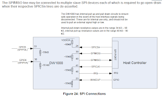
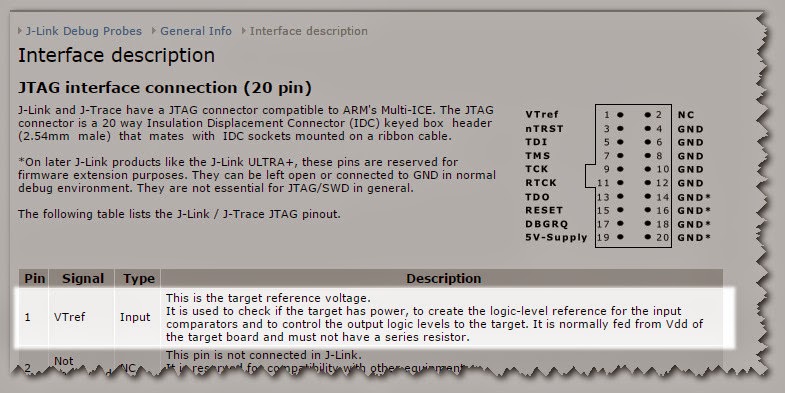
I thought the DW1000 I/O supply could be run at 1.8V, but it can’t. It’s 2.8V – 3.6V. There are separate 1.8V-optional supply pins for digital and analog circuits (to save power) but they can run at 3.3V. So for the time being, since the nRF51822 can run at 3.3V, the whole board will be 3.3V so all the I/O’s will be 3.3V. Later we will have to determine if running the nRF51822 at 1.8V for power saving is needed, then level shifting the signals connected to the DWM1000.I assume the Segger adjusts to the proper I/O voltage by means of its Vref pin.
—————–
I’m not sure how the SEGGER knows how to adjust, but I found this bit in the SEGGER documentation.
Notice the skip from workday #29 to #33. For the past three work-days and more I have been proceeding on plan B. Sadly this has not resulted in any code because I’m still trying to install a bloody tool-chain! (Tool chain, tool-chain, or tool-chain?) I’m frustrated and tired, and taking a break to write down what I have learned in the hope it sticks in my brain and comes in handy one day.
“One thing that amazes me is how nobody ever thinks to provide a conceptual model. There are lots of recipes, all of which become rapidly out of date. Nobody seems to understand that even a simple description of the objects, how they fit together, and what commands they implement, would so vastly simplify the process of understanding complex systems, as to enable people to figure out solutions for themselves, and eliminate most of the need for lengthy recipes.”
Turns out the Eclipse model is very flexible, and there are few general rules. Correction! There are general rules, but there are few general rules to which people universally adhere. Each tool-chain implementer has taken their own set of liberties with the intended architecture, and made certain assumptions, or put in extra configuration steps, to minimize the amount of adaptation work they have had to do.
Then of course there are different compiler chains, even for the same hardware. I already know that there are Gnu, Code-Sorcery, and Keil compilers that target ARM processors. Atmel has ARM tools too. Then there are all the plugins that know about details of a processor – like the Nordic chips with integrated BLE. So there are choices with benefits, and penalties.
——————
David responds:
Far from dropping off to sleep it was very interesting. But exhausting to imagine going through it. At least you have the knowledge and background to figure it out. I wouldn’t be able to – not even to start down the path.. What a huge effort. What is everybody else in the world doing to use these tools?
Here’s my plan:
Revise the DW demo code to make the port to TS06 as easy as possible
- Install Eclipse (in the manner prescribed by DW) and try to compile a minimal hello.c (“hello world”) program for the ST32F407 “Discovery” board I have in the cupboard. This will show that I can configure eclipse for an STM ARM chip. I was able to do that some months ago, so it ought to be reasonably easy.
- Reconfigure eclipse for the DW eval kit (EVK) and compile hello.c for the DW eval kit (EVK). Alas the EVK uses an ST32F105. There are substantial processor differences obviously, and I will have to figure out how to load and debug code on the DW platform. I’m hoping the move is simply a matter of specifying the different processor, and using a different in-circuit programmer/debugger (e.g. SEGGER).
- Compile DW’s demo program and see if I can get it to load and run on the EVK. In theory this ought to be easy because DW tell you how to do it, but I have not had an easy time with the eclipse setup documentation, so who knows how hard this will be in practice.
- Strip down the DW demo code to some form that could run on the M0. This means stripping out all the code that uses the LCD, switches and so forth. I will need a simple test program that can indicate that ranging is working OK. This will give me a test program that provably works with functional ranging hardware.
Create a minimal Hardware Abstraction Layer (HAL) for the TS06
- The first step is to configure eclipse to target a Nordic M0. Earlier this year I found this to be a real challenge.
- Create a new TS06 HAL that will allow the same hello.c program to run on the TS06, EVK and Discovery boards. It should be possible to have exactly the same program run on all three.
- Extend the TS06 HAL to talk to the DW module.
- Get the minimal DW demo code to run on the TS06
Do everything else
Today I started trying to install the eclipse IDE so I could compile and load the DW sample code on the evaluation system.
The document ECLIPSE IDE SETUP GUIDE that I have downloaded is out of date and the instructions simple do not work. They rely on Sourcery CodeBench Lite for ARM EABI. When you go to the sire you get this.
Sourcery CodeBench Lite releases for ARM EABI, ARM GNU/Linux, ARM AARCH64-Linux, IA32/IA64 GNU/Linux and ELF are no longer available.
I tried to download it from elsewhere and the virus checker claimed it was full of viruses.
Nordic announce support of some near-field charging standard.
I don’t understand what Nordic have done.
——————–
On Fri, Oct 31, 2014 at 8:56 AM, David Carkeek <dcarkeek@gmail.com> wrote:
There are a bunch of new things in this press release so I don’t understand it either. They say “magnetic resonance” and “spatial freedom” but then talk about pads and surfaces as though the device has to be resting on the surface. It s says “Out of Band” which I don’t understand and “up to eight devices”. Why couldn’t it be nine devices? Why do you need an SDK to make a charging system?
What I kind of think is that there a pad which is a kind of transmitting antenna that emits a signal to which a device resonantly couples over a distance that is not zero for the purpose of transferring energy for battery charging. Each device needs a channel (up to 8 are possible). That would be super cool if true. Need to read about Rezence. I might be completely wrong.
“The nRF51 Wireless Charging SDK is available today on a limited basis to lead customers.”
but “Engineering build of S120 and an updated nRF51 SDK is available today as a download for existing customers of nRF51822.”
Whom do I ask for the link? Not that I would know what to do with it after downloading.
On Fri, Oct 31, 2014 at 10:46 AM, Mik Lamming <mik@lamming.com> wrote
Following up on I’m assuming that the range is at best centimeters because it is near-field which drops off dramatically after a few wavelengths… doesn’t it? The frequency is 6.8MHz, so the wavelength is ~5cms? (Wrong 44.1 meters)
The interface standard supports power transfer up to 50 Watts,[1] at distances up to 5 centimeters.[2]
————————–
On Fri, Oct 31, 2014 at 11:29 AM, David Carkeek <dcarkeek@gmail.com> wrote:
Too bad it doesn’t work across a room, but still quite interesting. I watched about 5 minutes but I’ll have to finish it later.I’m somewhat ashamed to say I don’t know much about RF fields, near-field, and the relationship of wavelength to power transfer. The wavelength of 6.8 MHz is 44 meters according to the calculator. I wonder why that frequency was chosen. It must mess pretty badly with nearby radios.A Tesla coil can work at tens of feet, maybe hundreds of feet.
—————————–
On Fri, Oct 31, 2014 at 13:59 AM, Mik Lamming <mik@lamming.com> wrote
Ah MHz, not GHz! Yes – I agree. Doh. Good job you check all my math.
c = 300,000 = 3 * 10^5 kms/s = 3*10^8 m/s
6.8 MHz = 6.8 * 10^6Wavelength = (3*10^8) / (6.8 *10^6) = 44.1mIt’s only the first 5mins that are worth the time. The rest got out of my depth anyway. It just gave me a good feel for the strengths and weaknesses of near-field.


