I just read through the Nordic and RayTac manuals and discovered answers to what we were talking about today re. pin assignments for TS06.3

Here are the “standard” pin assignments for SPI, I2C and UART.  There are two SPI controllers, two I2C controllers, and one UART controller.  It is only possible to have three such “serial” devices active simultaneously.  I discuss this more below under “Controller conflicts”

First let’s collect up all the standard pin assignments that the the Nordic software assumes.

Standard Pins Assignments

SPI

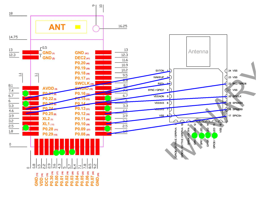
There are two SPI controllers SPI0, and SPI1.  The pin numbers are as follows.  The DW module should be connected to SPIM0
#define SPIM0_SCK_PIN       23u     /**< SPI clock GPIO pin number. */
#define SPIM0_MOSI_PIN      20u     /**< SPI Master Out Slave In GPIO pin number. */
#define SPIM0_MISO_PIN      22u     /**< SPI Master In Slave Out GPIO pin number. */
#define SPIM0_SS_PIN        21u     /**< SPI Slave Select GPIO pin number. */

#define SPIM1_SCK_PIN       29u     /**< SPI clock GPIO pin number. */
#define SPIM1_MOSI_PIN      24u     /**< SPI Master Out Slave In GPIO pin number. */
#define SPIM1_MISO_PIN      28u     /**< SPI Master In Slave Out GPIO pin number. */
#define SPIM1_SS_PIN        25u     /**< SPI Slave Select GPIO pin number. */

I2C

There are two I2C controllers.  Each controller uses two GPIO pins which can be any of the available GPIOs.
#define TWI_MASTER_CONFIG_CLOCK_PIN_NUMBER (24U)
#define TWI_MASTER_CONFIG_DATA_PIN_NUMBER (25U)

UART

Any four pins can be used for the UART.  The standard pins to use are:
#define RX_PIN_NUMBER  11
#define TX_PIN_NUMBER  9
#define CTS_PIN_NUMBER 10
#define RTS_PIN_NUMBER 8

ADC

I added in the ADC pins because they are special, and we might need the odd ADC pin for something.  The ADC uses a minimum of two pins.  One samples the input, and the other provides a reference voltage.  If we have any ADC needs then we will have to use:

  • either pin 23 or pin 17 for reference voltages.
  • pins 9, 10, 18, 19, 20, 21, 22, or 23 as inputs.

Because 9 and 10 are used for the UART, and 20-23 for the SPI0, we are left with 17, 18 and 19.

#define AREF0            17u      // ADC reference pin
#define AIN2             18u      // ADC sample pin #1
#define AIN3             19u      // ADC sample pin #2

Controller conflicts

It isn’t possible to have all five serial controllers active at the same time because they share address space. 

SPI0 and I2C0 share the same address space
SPI1 and I2C1 share the same address space
The UART has it’s own address space. 
So allowed combos are:

  • UART and 2 x SPI, or 
  • UART and 2 x I2C, or 
  • UART and 1 x SPI, and 1 x I2C.
There are various weasel words that allow other combinations, but we must have 1 x SPI for the DW, and 1 x I2C for the Coulomb counter.  Clearly I will have to figure out how to string other devices on the SPI bus with the DW.

Summary of suggested Nordic GPIO pin assignments

So pulling all this together we end up with the following constraints on pin assignments
#define                      0u
#define                      1u
#define                      2u
#define                      3u
#define                      4u
#define                      5u
#define                      6u
#define                      7u

#define RTS_PIN_NUMBER       8u      // UART
#define TX_PIN_NUMBER        9u      // UART
#define CTS_PIN_NUMBER      10u      // UART
#define RX_PIN_NUMBER       11u      // UART

#define                     12u
#define                     13u
#define                     14u
#define                     15u
#define                     16u


#define AREF0               17u      // ADC reference pin
#define AIN2                18u      // ADC sample pin #1
#define AIN3                19u      // ADC sample pin #2


#define SPIM0_MOSI_PIN      20u     /**< SPI Master Out Slave In GPIO pin number. */
#define SPIM0_SS_PIN        21u     /**< SPI Slave Select GPIO pin number. */
#define SPIM0_MISO_PIN      22u     /**< SPI Master In Slave Out GPIO pin number. */
#define SPIM0_SCK_PIN       23u     /**< SPI clock GPIO pin number. */

#define I2C_CLK             24U     // I2C clock pin
#define I2C_DAT             25U     // I2C data pin

#define                     26u
#define                     27u
#define                     28u
#define                     29u
#define                     30u
#define                     31u

Other pins that can be connected to any GPIO are
DW_IRQ
DW_RSTn  — this may not be needed
DW_WAKEUP

SLAVE_SEL x N  for any other SPI devices beyond DW which uses pin21

All other pins can be assigned to LEDS, or BUTTONS


Another minor, yet significant step forward today.  I have a trivial program echoing packets between my Android and the TS06.2.   The same program (nRF UART) is allegedly available on the iPhone!

  1. The TS06 sets up all the BLE services, and then advertises its presence to the world.
  2. The Andoid is told to discover what’s out there so I can select it as the target for echoing packets.
  3. Then I type in a few words and send them – the TS06 echoes them back.  
  4. Then I disconnect and reconnect to show it wasn’t a fluke (though it probably was!)

The less encouraging news is below:

Invoking: Cross ARM GNU Print Size

   text   data    bss    dec    hex filename
  71068 2268   1196  74532  12324 BLE_UART_C_nRF51822.elf

It continues to be a long haul.  I have installed SDK 8.0.0 and have been slowly recompiling all my various bits of test code.  Each little test program reveals some new gotcha that I didn’t quite understand, so I guess it’s kind of useful.  Why recompile it all?  I guess I want to be sure that everything works as before, in case there are hardware issues.

The good news is that the new SDK has bits of useful support code that I’m able to use, and thus throw away my own code which has a lot less testing.

Another day or so and I should be back to writing new code that matters.

The last two test programs went a lot faster than I anticipated.  I’m done.  So now I can get back to developing code again.

Recall that Nordic has a “soft-machine” that runs in high memory that provides the BLE functionality.  That eats up a bunch of memory, and our application has to make do with what’s left over.  The application uses a Nordic API that knows where all the entry points to the SM are located in memory.  So the SDK API and the SM are a matched pair.

I have been writing code using SDK V6.1.0.0 without a soft machine loaded because my code has not used BLE yet.  
While I was in SB I got a couple of hours to futz around with TS06.2, and thought I’d pursue the BLE thread a bit.  If the ranging works then I’ll want to write the ranges to the cloud somehow, and it makes sense to use some kind of BLE transport mechansim to do that.  So I thought I’d make a really dumb BLE program that emulated a serial port connection.  Ha!!

Since I last installed the Nordic devkit it has gone through two major releases.  V6 is now V8.  In particular the BLE soft-machine that you load into high memory has moved on too.  Indeed I can’t actually find a matching soft-machine any longer.  So I pretty much have to upgrade the SDK.
SDK 8 codebase is organised quite differently, so I’m glad I didn’t have any BLE code to port across.  On the other hand, there are no instruction for installing V8 under eclipse.  So I made my best attempt and hey presto, none of my programs work under V8.  
So it looks like I have another diversion to work around.


//Mik

The pin connection spreadsheet is here.

I think it should look like this.

Test program


  1. Go to the TESTING directory
  2. If you don’t have it installed already, download and install JFlashLite_V485a.zip
  3. Download the test program TS06_CHECKOUT_C_nRF51822.hex
  4. The UI to JFlashLite is tedious but easy.  Make sure to specify the correct processor using the pull-down menu.
  5. The program should start automatically, but if it doesn’t, then power-cycle. 

OutputThe program loops performing the following 4 tests:

  1.  All the LEDs should come on for 3 seconds.  N.B. LED on pin 0 marked ‘X’ in the photo, is broken on my board, and should be on.
  2. It tries to access the DW chip, and get the chip ID.  If it suceeds it “floods” the LEDs till they are all on in a clockwise direction
  3. It tries to read the DW temp, and battery gauge.  If it suceeds it “un-floods” the LEDs till they are all OFF in a counter-clockwise direction.
  4. The it tries to prime the transmit buffer with test data,  If this works it sets the bottom TWO LEDs
  5. Then it tries to issue a ‘transmit’ command.  If this works then the bottom FOUR LEDs are set.
  6. If the transmission finishes and an interrupt is raised then it sets the bottom SIX LEDs.
  7. To signal the end of the test it ripples the LEDs to and fro 5 times.

Then it returns to step #1

    TS06.3

    Goals in priority order

    • Establish our process for board replication. That, by itself, is plenty of work, and a lot of unknowns.
    • Evaluate alternative components for TS06.4 

    Steps

    I’m all for keeping the TS06.3 iteration simple. I propose we only fix immediate shortcomings, so we can focus energy on setting up our production process.

    1. Clean up what we have right now – pin assignments, leds, connectors, jumpers.
    2. Not add any new functionality that demands extra software, because I think we will iterate on the h/w again before I have ranging, BLE uploads, and simple PC data display working.
    3. The exception to the above is, maybe to provide hooks so we can measure power consumption, or you can explore power supply/energy harvesting
    4. Decide on our board design/production process, so we can bang out new boards quickly, and confidently. Would a reasonable target be to go from proposed change to flashing the board in under a month?
    5. Replicate a few more (N~8) units for us both to play around with.

    Other things to discuss

    • Smaller? Only to go smaller if it just happens as a result of cleanup, not to make it a goal?
    • Enclosure?  None?
    • Experiment with a less clunky JLINK connector. e.g. Plug-of-nails?
    • Above connector externalizes POW, GND, I2C, USART, 2nd SPI to allow for hacky pre-TS06.4 experiments
    • Remove most of the jumper connections – especially around the DW which doesn’t really need them. Maybe only scratch-able/solderable links?
    • PSU – do we need to experiment with anything?
    • Support for DC’s energy-harvesting experiments?
    • Provide battery option to allow for quick-and-dirty ranging experiments. Could we use a USB battery pack if the USB connector was different?
    • Colored LEDs on unused Nordic pins?

    TS06.4

    I’m optimistically calling this 6.4, but there might be other iterations required before we get here. It just here to set a context for discussing TS06.3

    Goals in priority order

    1. Power management – enhancements to drive down power usage, and simplify the user’s recharging experience.
    2. More data storage (this may be #1)
    3. Another step down in size towards wear-ability.
    4. Experiment with potential enclosures
    5. IMU

    TS06.5

    The first version we try to wear for extended experiments.

    Temp and Voltage

    Temp = 87.01. Volts = 3.01
    Temp = 88.14. Volts = 3.00
    Temp = 87.01. Volts = 3.00
    Temp = 87.01. Volts = 3.00
    Temp = 88.14. Volts = 3.01
    Temp = 88.14. Volts = 3.01
    Temp = 88.14. Volts = 3.00
    Temp = 88.14. Volts = 3.00
    Temp = 88.14. Volts = 3.01
    Temp = 87.01. Volts = 3.00
    Temp = 87.01. Volts = 3.01
    Temp = 88.14. Volts = 3.00
    Temp = 88.14. Volts = 3.00
    Temp = 88.14. Volts = 3.00
    Temp = 87.01. Volts = 3.00
    Temp = 88.14. Volts = 3.00
    Temp = 88.14. Volts = 3.00

    Write a short data packet

    I think I may be transmitting a short text packet, but I have no way of knowing if it is really going into the ether.

    Today I manged to compile the DW API, and ran a couple of simple test programs.  

    One uses the API to check that the DW module is awake, and is the correct version.  It replied:

    SEGGER J-Link GDB Server V4.98b – Terminal output channel
    deca0130  <-  this is good!

    The second test attempted to flash the LEDS connected to the DW module.

    This example uses a dumb two-line test program using just a bit of Nordic library, and some DW library.  The code size is:

    arm-none-eabi-size –format=berkeley “SPI_to_DW_C_nRF51822.elf”
       text   data    bss    dec    hex filename
      52728   2552    768  56048   daf0 SPI_to_DW_C_nRF51822.elf

    How to interpret the size data

    text is the size of the code in flash.
    data is the amount of initialized data. It also lives in flash.

    bss is where all the variable data lives which is RAM.

    So I already have used about 55K of 256K of flash and 0.75K of 16K of RAM.  However the BLE softmachine is not loaded and that consumes 88K flash and 8K RAM.

    So the current freeboard is:

    Flash: 256-(88+55) =  113K
    RAM: 16-(8+0.75) = 7.25K  — fortunately there is a 32K version

    Yesterday I managed to prove I could both read and write to the DW.  My code uses an interrupt routine, so that, in theory anyway, the processor can be doing other stuff while the transfer is in progress.  This may prove to be a small gain, and in any case I discovered that DW do not use interrupt-driven SPI.  Indeed they implement a mutex that turns off interrupts from the DW module while the transfer is in progress, which I’m curious about.

    The other snag is that their SPI routine transfers the command, and data bytes in separate buffers.  I could rewrite my interrupt routine to match their calling protocol, but that’s going to be a bit fiddly and will undoubtedly introduce some bugs.  So I decided to simply copy the two chunks of DW data into a separate buffer, and call my usual one-buffer routine.  I did that getting it to work at all is higher priority, and I can rewrite it later to save the extra buffer space.
    OK, so the next step is to port a little more code over and see if it can drive the DW through my SPI routines.

    David: 


    Remember that Nordic have released their version with 32K RAM and Ray-Tac have sample modules available. Do we want to order some?
    And if we order more modules so we want to get some of the nano versions which are much smaller? But the nano version doesn't have an antenna. I think the idea is to use a PCB antenna, so to do any RF stuff we have to lay out a board.
    Speaking of laying out a board, we can do that as soon as we have module connections that we know will work. I think we're getting close to it.

    Mik:
    I think RAM may be a problem, but I reckon we will run out of program space before we run out of RAM.   I wouldn't bother getting any new modules until we get closer to running into the problem because there may be even better options available by then.  

    As for going smaller: I think we should just go with the modules we have.  They work.  I think our priority is getting the ranging software to work.  If and when it does work, then we will have software that can serve two purposes in the next round of hardware:
    1. We can checkout the new hardware (instead of trying to debug possibly flaky hardware with possibly flaky software)
    2. We can create some ranging benchmarks against which to measure our own antenna designs.

    Module connections:   Here is what I know about the connections  ( see blue box)

    Summary:
    • Some of the DW pins that we have connected to GPIOs are not needed. I think they can float or be be tied hi/lo to save leakage.
    • The DW SPI and IRQ lines can be connected to any pins that make layout easy – it just means changing a defined constant for me.  I have made suggestions.  
    • I don't yet know is RSTn is actually required – I would suggest connecting it via a jumper.  It can probably be tied hi/low?

    //Mik

    On Mon, Apr 13, 2015 at 10:36 PM, David Carkeek <dcarkeek@gmail.com> wrote:

    I can't imagine going through all that. How do you do it? 

    Remember that Nordic have released their version with 32K RAM and Ray-Tac have sample modules available. Do we want to order some?
    And if we order more modules so we want to get some of the nano versions which are much smaller? But the nano version doesn't have an antenna. I think the idea is to use a PCB antenna, so to do any RF stuff we have to lay out a board.
    Speaking of laying out a board, we can do that as soon as we have module connections that we know will work. I think we're getting close to it.

    On Mon, Apr 13, 2015 at 10:06 AM, Mik Lamming <mik@lamming.com> wrote:

    You might wonder what the hell I have been doing all this week.  

    I think we can confidently predict TS06 will run out of program space early.  
    It has to have BLE drivers, and DW drivers as well as all the other sensor stuff, and analysis software.  While we wait for a Nordic processor with more memory I will probably have to partition the code development – i.e. develop and test parts of the code independently, and finally cherry-pick and squeeze bits of code to make the TS06.  (Of course, the BeSpoon module has the advantage that a lot of the code that is outside the DecaWave module is inside the BeSpoon module, but who knows if BeSpoon will last much longer?) 
    I tried partitioning thing with TS02..5.  But the toolkit was more primitive and made it hard to share code between different independent threads of development.  For example, I had a code base that was designed to explore and test the hardware, and another for the networking, and another that integrated parts of the others to make TS.  But it was so hard to partition the code between the two different applications, and back it up each night.  Fortunately the Atmel 256K processor came along, and so I was able to do everything in one module with some squeezing.  Indeed the final code base for TS05 is actually called HWTest rather than TS!  So the code contains a lot of stuff that isn't really needed, and of course soaks up valuable memory.
    I already have several threads going that I am trying to keep separate for simplicity and speed.  But keeping all the source libraries (DW, Nordic) separate and shareable took some more study, and created it's own snags.   Also I will need to keep DW and BeSpoon developments separate.  Then I need to be able to keep the developments for each board definitions separate.
    So organizing the development tools has taken way more time than I ever thought possible – exacerbated by my own ignorance.
    I think I have it kind of organised now, but time will tell.  I'm also backing it up to a git repository so I can move the code base between desktop, and laptop in anticipation of going to the UK.
    It is truly amazing how much time this kind of stuff soaks up.