I just realized that I didn’t fully understand a feature of the DW hardware.  Although they talk about responding after a fixed delay, they don’t exactly do that.

The ranging process involves sending a packet on a round trip to a peer, which holds the packet for a fixed, and known period before sending it back to the sender.

The hardware will transmit the packet when a system counter reaches a specified value Ttx  The counter is 40 bits long, and wraps every 17 seconds, so it increments a bit every ~16 picoseconds. The same kind of system counter is used to notice the arrival time, Trx,  of the packet demanding the response.  So you would think that Ttx =Trx + fixedDelay.

In fact they use  Ttx = (Trx + fixedDelay) & 0xFFFFFFFE00  which potentially lops about 8ns off the arrival time.  i.e. 2+ meters!   Why do they do this, and why doesn’t it matter?

Here’s my theory.  The actual time we want the packet to leave the antenna is going to be a little after the radio streams out the signals, because they have to crawl down to the antenna.  So there is an antenna delay.  So the radio needs to send the bits out a little early so they leave the antenna at the desired instant.

Now perhaps the chip can’t do carry-arithmetic, so they just make it easy to OR in the antenna delay. In any case the don’t bother unduly about getting the transmit time correct.  All they need to ensure is that they have delayed long enough for the receiver to wake up and start listening.

Ttx = antennaDelayTime + (Trx + fixedDelay) & 0xFFFFFFFE00

Now I’m not sure if the actual transmit time stamp is simply computed and taken as fact, or if some analog magic causes the system counter to get copied at the critical moment.  I suspect the former.

Adding in the antenna delay could produce a value that’s larger than 40 bits.  But the system counter wraps at 40 bits, so the start time is masked at 40 bits too.

Ttx = (antennaDelayTime + (Trx + fixedDelay) & 0xFFFFFFFE00) & 0xFFFFFFFFFF

A potential snag with this mechanism is that something could slow up the host microprocessor from calculating the transmit time.  If that takes so long that the transmit time passes then the game is over, and everything has to start over.
In order to run a .hex file you don’t need to install Eclipse or any of that crap.  You just need to install the “flasher”, erase the memory, and then flash the test program.

Flashing test program #1

  1. Go to the TESTING directory
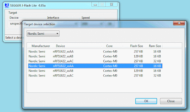
  2. If you don’t have it installed already, download and install JFlashLite_V485a.zip
  3. Download the test program Blinky32k_C_nRF51822.hex
  4. The UI to JFlashLite is tedious but easy.  
  5. Make sure to specify the correct processor using the pull-down menu. nRF51822_xxAA

  6. Erase the memory first time around.
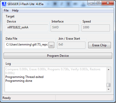
  7. Set the “Data file” field to point at the test program .hex file
  8. Press “Program Device”
  9. After the flashing process, the program might not start automatically (probably because there is a fossil breakpoint at “main”).  If it doesn’t start, then power-cycle the board. 

    while (true)
    {
     LED_clearAll();
     nrf_delay_ms(500);
     LED_setAll();
     nrf_delay_ms(500);
     LED_clearAll();
     for (int i = 0; i < LEDS_NUMBER; i++)
        {
            LEDS_INVERT(1 << leds[i]);
            nrf_delay_ms(500);
        }
    }

    Test program #2

    1. Plug the USB port into the PC – a new COM port should be created
    2. Open your favorite terminal-emulator (e.g. Putty?)
    3. Set 38400, 8, 1, parity:none, flow-control:none
    4. Download and flash the test program Blinky32K_USB_C_nRF51822.hex

        while (true)
        {
        LED_clearAll();
        nrf_delay_ms(500);
        LED_setAll();
        nrf_delay_ms(500);
        LED_clearAll();
        for (int i = 0; i < LEDS_NUMBER; i++)
            {
                LEDS_INVERT(1 << leds[i]);
                nrf_delay_ms(500);
            }
    ts_uart_init();
    TS_TRACE(“rn———–rn%s HW:%s SM:%s SW:%s(%s %s)rn”,
    MANUFACTURER_NAME, DEVICE_NAME, SDNAME, SERVICE_NAME, __DATE__,
    __TIME__);
        }

    JFlash Log

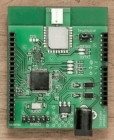
    Here is what the jFlash log looks like when it downloads to the TS06.2
    Erasing nRF51822_xxAA via SWD-Interface@1000kHz 
    Erase Thread started.
    Device “NRF51822_XXAA” selected.
    Found SWD-DP with ID 0x0BB11477
    Found Cortex-M0 r0p0, Little endian.
    FPUnit: 4 code (BP) slots and 0 literal slots
    CoreSight components:
    ROMTbl 0 @ F0000000
    ROMTbl 0 [0]: F00FF000, CID: B105100D, PID: 000BB471 ROM Table
    ROMTbl 1 @ E00FF000
    ROMTbl 1 [0]: FFF0F000, CID: B105E00D, PID: 000BB008 SCS
    ROMTbl 1 [1]: FFF02000, CID: B105E00D, PID: 000BB00A DWT
    ROMTbl 1 [2]: FFF03000, CID: B105E00D, PID: 000BB00B FPB
    ROMTbl 0 [1]: 00002000, CID: B105900D, PID: 000BB9A3 ???
    Debugger initialized successfully.
    J-Link: Flash download: Total time needed: 5.550s (Prepare: 0.103s, Compare: 0.000s, Erase: 5.440s, Program: 0.000s, Verify: 0.000s, Restore: 0.007s)
    Erase Thread exited 
    Erase done

    Downloading C:UserslamminggitTS_repoBlinky_C_nRF51822NOSD_TS06.2Blinky_C_nRF51822.hex to nRF51822_xxAA via SWD-Interface@1000kHz 
    Programming Thread started.
    Device “NRF51822_XXAA” selected.
    Found SWD-DP with ID 0x0BB11477
    Found Cortex-M0 r0p0, Little endian.
    FPUnit: 4 code (BP) slots and 0 literal slots
    CoreSight components:
    ROMTbl 0 @ F0000000
    ROMTbl 0 [0]: F00FF000, CID: B105100D, PID: 000BB471 ROM Table
    ROMTbl 1 @ E00FF000
    ROMTbl 1 [0]: FFF0F000, CID: B105E00D, PID: 000BB008 SCS
    ROMTbl 1 [1]: FFF02000, CID: B105E00D, PID: 000BB00A DWT
    ROMTbl 1 [2]: FFF03000, CID: B105E00D, PID: 000BB00B FPB
    ROMTbl 0 [1]: 00002000, CID: B105900D, PID: 000BB9A3 ???
    Debugger initialized successfully.
    J-Link: Flash download: Flash programming performed for 1 range (39936 bytes)
    J-Link: Flash download: Total time needed: 0.870s (Prepare: 0.108s, Compare: 0.008s, Erase: 0.000s, Program: 0.741s, Verify: 0.002s, Restore: 0.009s)
    Programming Thread exited 
    Programming done

    Troubleshooting

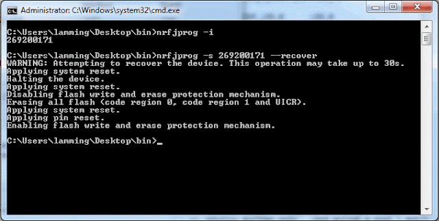
    If the new module won’t erase, or flash correctly then it may be that the memory is protected.  Here is how to remove that protection.

    I put a zipped directory called nrfjprog.zip out in the usual place.
    Inside is a “bin” directory.
    Copy that directory somewhere – your desktop for example.
    Open a command window on the bin directory.
    Type the command nrfjprog -e
    Inline image 1

    Then try erasing and flashing again using jflash

    If that doesn’t work, then do the following:

    1. Get the serial number of your jLink, e.g.
      >nrfjprog -i269200171

      It should match the number printed on the label on the back of your jLink box.

    2. Reset everything
      > nrfjprog -s <jLinkSN> –recover

    Went to bed exhausted last night.  I’m really having a lot of trouble getting the ranging to work.  So far I can send and receive packets.  I think I can send packets after a fixed delay, but I can’t seem to receive them correctly.

    Some of my problems are clearly just not understanding how to configure the chip for the subset of stuff I need to do.  Then there are illogical behaviors, and frankly — chip bugs.

    Status bits are set in the wrong chronological order.

    This sequence of trace messages shows the problem.  I’m joining battle here at the point when one TS has sent a “ranging init” packet to the other.  A ranging-init packet is the “serve” in the ping-pong game of packet exchanges between the two peers).  After sending that packet the radio goes to sleep, an I’d expect to get notification of the packet having been finally sent, but in fact I get told (very reasonably) that the radio has woken up: (SYS_STATUS_SLP2INIT); that the clock has locked up OK: ( SYS_STATUS_CPLOCK); that a packet preamble has been successfuly decoded (SYS_STATUS_RXPRD ); that the clock has lost lock again (SYS_STATUS_CLKPLL_LL ); and that the rest of the packet timed out (SYS_STATUS_RXSFDTO).  All of this gets reported at a higher level in the DW IRQ handler as a “receive error” (DWT_SIG_RX_ERROR)

    After all that is said and done I get to hear that my original transmission has completed (DWT_SIG_TX_DONE).  This bizarre sequence makes it difficult to build a rational state-machine, and indeed my code (and I actually) get’s confused and hangs up.

    (25931) ranger_rxcallback DWT_SIG_RX_ERROR
    SYS_STATUS_IRQS SYS_STATUS_CPLOCK SYS_STATUS_RXPRD SYS_STATUS_SLP2INIT SYS_STATUS_CLKPLL_LL SYS_STATUS_RXSFDTO
    LISTENING_FOR_RANGE_INIT_RESPONSE
    (25932) ranger_txcallback DWT_SIG_TX_DONE

    It isn’t even possible to reply to every ranging-init packet

    The technique for measuring time of flight is to note the value of a 40-bit timer as a ranging-init packet leaves the antenna.  The peer receiver gets the packet, and hangs onto it for an agreed amount of time before sending it back to the sender.  Believe it or not, that’s a relatively long time – 150ms.  When it gets back to the original sender’s antenna, the clock is read again, the tx and rx times compared and range calculations happen.
    Buried deep with the chip is a very fast clock that time stamps the packets going out.  The clock is only 40 bits wide, and so it wraps around quite often.   Each bit in the 40-bit timer represents 16 psecs, so the counter wraps every 16 * 2^40 = 17 seconds.   The timer keeps running all the time and is never zeroed, so if the transmit time is expected to wrap before the reply might conceivably arrive, then the whole operation is aborted.   This results in the confusing message “too late”. Of course restarting the ranging sequence burns power.

    WAIT_TX_RESP_DONE
    (2839) listener_rxcallback DWT_SIG_RX_ERROR
    SYS_STATUS_IRQS SYS_STATUS_CPLOCK SYS_STATUS_RXPRD SYS_STATUS_SLP2INIT SYS_STATUS_CLKPLL_LL SYS_STATUS_RXSFDTO
    LISTENING_FOR_RANGE_INIT_RQ
    (2840) listener_rxcallback DWT_SIG_RX_ERROR
    SYS_STATUS_IRQS SYS_STATUS_CPLOCK SYS_STATUS_RXPRD SYS_STATUS_SLP2INIT SYS_STATUS_CLKPLL_LL SYS_STATUS_RXSFDTO
    LISTENING_FOR_RANGE_INIT_RQ
    too late

    Chip is buggy

    There are clearly undocumented issues with the chip, that are only revealed in the code.  I’m not sure that I have actually hit these bugs yet, but I decided to use their IRQ handler which appears to contain fixes for the bugs, albeit with a lot of extra “interrupts off” handling code.  
    //fix for bug 622 – LDE done flag gets latched on a bad frame
    // bug 634 – overrun overwrites the frame info data… so both frames should be discarded
    //bug 627 workaround – clear the AAT bit if the ACK request bit in the FC is not set

    The paste I used was too old. But I have overcome that problem for the time being. I had a new container of paste (it looks identical to the small one they showed in the Sparkfun video) that I was planning to use. I have had it for a year, but I thought it might be OK since it was wrapped in plastic, and had a seal on the top of the jar. But when I took off the seal the lump of paste at the bottom of the container was hard as a rock. Therefore I used one of the three full ChipQuik syringes I have. The paste looked fine and flux was evenly distributed throughout the solder powder. However, it didn’t melt properly. The balls clumped up or just didn’t melt at all in some places, but other areas were OK. Obviously the flux composition changes over time. After adding flux and touching it up with an iron all looks good or acceptable.
    I spent the first part of today bringing up the power supplies. There were several board design errors.
    – U2 SHDNn needs to be pulled high until the uC comes up.
    – U3 SHDNn needs to be pulled high until the uC comes up.
    – U3 Vin needs a 10uF cap
    – U3 voltage divider must connect to VOUT instead of VIN
    I tied SHDNn on both devices to their Vin, forgetting that the signals also goe to the uC module. Therefore I put 4V on those module inputs while there was no voltage at the Vdd pins. This forward biased the ESD diodes on the nRF51822 and supplied power to the rest of the chip, enough that some of the LEDs came. The module could be damaged, but it might still be OK, since we already did basically the same thing once on the perf boards. If it’s damaged it will not be hard to replace.
    Now both power supplies are working. The (eventually) solar cell powered regulator is supposed to start at 250mV but it doesn’t start until there is 800mV on the input and it needs at least 1A to start when it is feeding the second regulator. Once it starts the current drops to nothing. When there is a battery on the output (of the first regulator) the starting current won’t be a problem; I wonder if the 250mV start voltage is dependent on a battery being present on its output. It shouldn’t be. So why is the starting voltage so high? Questions for the LT apps engineer.
    I’m not sure how to set up the main regulator optimally. It’s working with the values shown in the datasheet. I don’t understand the theory of operation where poles and zeroes are discussed. I didn’t get much about transfer functions in school and there was no reason to learn about it later.
    Going to https://en.wikipedia.org/wiki/Pole%E2%80%93zero_plot reinforces my feeling of ignorance. I thought I wanted to use LTC3335 for the next design; I see that it doesn’t have a compensation network connection so I wouldn’t need to worry about the network design. But the LTC3335 needs 1.8V input voltage so using a small solar cell wouldn’t work with it. To use a solar cell would require two regulators as in the present design. An additional issue could be that the LTC3335 can output only 50mA, and the DW module receive current is 160 mA. If the DW only needs high current for a few hundred uS then a big cap might be adequate. The LTC3335 is perfect for powering from a coin cell. Maybe there can be one design for anchors and another for tags. But tags need the solar power more than the anchors.
    For now it won’t hurt to find out the optimum values for the LTC3107. Anyway, it’s working. Now I can put in the jumpers to turn on the modules.
    I am behind schedule at work. I think I need to go in tomorrow, and there is a special meeting called for 10:30 AM Monday morning that I need to attend, so I should wait at least until Tuesday to go to SF. 

    Reading the blurb for the RIGOLDS1054Z I felt quite inspired by the possibility of learning some cool stuff.

    Suppose one set up the scope to measure power consumption over a wide range from nA to mA.  I don't see how that can be possible, but perhaps a real-time trigger could change the sensitivity?
    Suppose that it could be triggered with a GPIO, and also that other GPIOs could be used to mark precise places of interest in the trace.
    Obviously looking at the scope trace would be informative.
    IMHO the win in this process is being able to set up recipes for particular measurements that could be used over and over without a lot of hassle to set each recipe up.  I'm sure this is probably SOP in the industry.
    So one could set up recipes for different operations (like listening, or sending a ranging message) , and easily switch between them as the code was refined to gauge improvement.
    Suppose the capture buffer was big enough to capture a whole cycle of operations spanning perhaps a second, e.g. discovery through ranging and the distribution of the new range data to peers.
    Further suppose that the trace data could be uploaded to the PC.  One could:
    1. calculate the area under the graph – the actual units are not important, because we care about differences
    2. traces could be superimposed to spot subtle differences and problems.


    //Mik

    On Sat, Jul 11, 2015 at 10:40 AM, David Carkeek <dcarkeek@gmail.com> wrote:

    Scope is scheduled to arrive on Friday by UPS. Since it's going to my PO Box I might not be able to get it until Monday. I could probably ask for it to held at the UPS depot in Sunnyvale if I really need it next weekend.

    A Picoscope would be perfect for you. Even the base model decodes SPI and I2C, and the 10 MHz model ($149 with two probes) has plenty of bandwidth for looking at SPI/I2C/JTAG.

    ———- Forwarded message ———-
    From: <orderstatus@tequipment.net>
    Date: Sat, Jul 11, 2015 at 9:54 AM
    Subject: Your TEquipment.NET Order Has Shipped! – Order# A075652
    To: dcarkeek@gmail.com
    Cc: dcarkeek@gmail.com

    205 Westwood Ave | Long Branch, NJ 07740 | 1-877-571-7901 | 732-222-7077 | 732-222-7088 (fax)

    TEquipment.NET

    Order #A075652
    07/10/2015
    Cust# 052380C

    Thank you for shopping at TEquipment.NET!

    Your package shipped on 07/10/2015, and a tracking number has been generated.
    In order to reduce handling and improve our shipping time, we now transport many of our packages directly to regional UPS/FedEx hubs. This may result in a short delay in finding your tracking number on their website. Rest assure that your package is on its way.

    Please see below for your order information and tracking number.

    SHIPPING SUMMARY:
    Myself
    Ship To: DAVID CARKEEK
    1750 LUNDY AVE #612871
    SAN JOSE, CA 95161-7116
    US
    4084723787
    Shipping Method: Ground
    Item/Description Qty Carrier Tracking#
    Primary Warehouse:
    RIGOLDS1054Z
    RIGOLDS1054Z

    50 MHz Digital Oscilloscope with 4 channels plus 12 Mpt memory, 1 GS/s sampling rate.

    1 UPS 1Z6619070373403218
     

    To log in to see your complete order status, including any items not on this shipment, please visit: https://www.tequipment.net/service/order/

    Thank you again for shopping at TEquipment.NET. We appreciate your business and look forward to serving you in the near future.

    Your Customer Service Team,
    We are here to help you.

    TEquipment.NET
    205 Westwood Ave
    Long Branch, NJ 07740
    1-877-571-7901 – Toll Free
    732-222-7077 – Local Tel
    732-222-7088 – Fax

    I’ve been trawling through the DW code all day, trying to figure out what the **** it is doing, and how it is doing it.  It took me a while to discover that there are two state machines that run in parallel. Of course the state names are similar, just to confuse things.  There is a state machine that keeps track of the SOC states, and then there is another state machine that keeps track of the ranging app.
    The state machine for the device initiating the ranging, is different from the SM for the node being ranged.  Rather than making two distinct SMs they combined them into one, and parameterized the states with “tag”, “anchor”, and “listener”.  Their ranging protocol exchanges 6 distinct packets which you would think would cause the SM to cycle through at least 6 extra states to keep track of the phases… but oh no.  There is a “prepare to send packet state”, and a “prepare to receive packet state”, both of which are parameterized with the packet type.  Bottom line is that the processing from some of these states has multiple combinations of option, and goes on for pages.  To understand which thread the code takes, I have to keep track of all the parameters in my tiny head.
    And of course it’s hard to trace through the code in the debugger, because it is a real-time system with lots of critical sections that time out.
    I am actually finding bugs in the code, so I do wonder how other folks have got on.  The basic timer code only handles a 5 second delay.  Any other parameter causes random results because the person that wrote it didn’t understand that you can’t shift a floating point number right 12 places and expect the same thing to happen as if you did it to a fixed point number.

    I’m of the opinion that the person who wrote this code wasn’t very experienced because it’s messy and  poorly structured.

    The DW status register has lots of status bits, that get set in what seems like a random order.  Sometimes condition A is asserted first, and sometimes condition B.  This means you have to write code to handle all possible sequences.  
    So I’m throwing away whole modules of code and building my own state machine, so I make sure I understand what’s going on.  It probably won’t work, but at least I will discover (the hard way) why they have all these subtle fiddly bits in their code.  And if it does work my code should be a lot cleaner because I don’t need to address all the demo options that complicate every touch and turn.  No wonder the Pozyx people used the same processor – they probably don’t understand how all the code works either.
    So no tangible progress, but at least I kind of understand the code more. 
    Cypress FRAM
    It's very interesting. Wouldn't it be only 500kB though? The density has to improve a lot before we could consider it for data storage.
    ————

    I was thinking of a couple of things:

    • There is a long-term data storage challenge, but saving stuff to a uSD card is thristy work.  To make sure nothing get's lost you have to write often.  Writing partial-pages is bad because the whole page has to be erased (v. expensive as I understand it) and re-written.  So you get to save power at the risk of losing data occasionally.   The alternative is to have a non-volatile FRAM cache.
    • The other challenge is on-board signal processing, and pattern recognition.  The technique is to build a tree-structured pipeline of filters that makes a single pass over the data.  The windows can get large and the intermediate results are cached to avoid unnecessary read/writing.  Obviously there isn't enough RAM to do much of that, but 500kB could make a difference. 
    Too early to think about much yet, but worth keeping an eye on options.  Does the new Nordicchip have the ability to extend it's address space with FRAM?  Can code be run from FRAM.  Code runs faster out of normal RAM.

    //Mik

    On Thu, Jul 9, 2015 at 9:26 AM, David Carkeek <dcarkeek@gmail.com> wrote:

    It's very interesting. Wouldn't it be only 500kB though? The density has to improve a lot before we could consider it for data storage.

    On Thu, Jul 9, 2015 at 9:06 AM, Mik Lamming <mik@lamming.com> wrote:

    Remember that I said we probably didn't need the WAKEUP signal.  I'm so glad you ignored me.   Today I managed to put the DW into a deep sleep, from which it was supposed to wake up after 5 seconds.  It didn't.

    Worse still I couldn't get it to wake up by resetting it.  
    The manual says that another way to wake it up is to hold the Chip Sel low for 200uS and read a whole bunch of data.   That didn't work
    So I was left with the WAKEUP line, which has to be held high for 200 uS.  Fortunately this worked.

    I thought I had a door stop for a while!

    //Mik
    Pozyx looks like an obvious repackaging of the EVK1000.  It amazes me that DW didn’t do this themselves at the start.  They could have had a whole bunch of people developing stuff a year ago if they had.
    I found it useful to measure pozyx and BeSpoon against our requirments, to see how much further along they are than us.
    I think this raises the short-term bar for us quite a bit, but doesn’t change anything other than the speed with which I need to get stuff working.  
    The holy grail right now is “wearability”, followed by ease of installation, and maintenance.   If we can really make something that is wearable for long periods, then I think we still could have something unique and valuable – but the race is on.  Only if we can get below the “24×7 wearable” threshold do we (and others) get to run experiments that will uncover non-obvious opportunities that I’m sure are there for the picking.
    • Wearable => small, nay tiny!
    • 24×7 => ultra-low-power => clever protocols
    • Easy/convenient to install => battery powered, or energy harvesting (or doesn’t hog sockets)
    • Easy to maintain => batteries don’t go flat, and doesn’t get confused by being moved
    • Can reliably communicate with support systems (apps, database, cloud, …)  in close to real time
    • I’d like to say “inexpensive”, but all hardware in inexpensive eventually
    • Non-stigmatizing – better improve your image, rather than v.v.
    • UI has to be physically easy to use (feedback is obvious, and input is easy to generate with high confidence)
    • Calibrated => the raw data has to have meaning after the hardware is defunct
    • Software makes it easy for the average programmer to write an analyzer
    • Private and secure
    • Sticky – does something indispensable